Printed Circuit Boards (PCBs) are the foundation of modern electronics, providing the necessary electrical connections between components. A reliable PCB manufacturer follows a precise manufacturing process to ensure quality, efficiency, and performance. Understanding this process helps engineers and designers optimize their PCB designs for better functionality and cost-effectiveness.
1. PCB Design and Layout
The first step in PCB manufacturing is the design phase, where engineers create a schematic and layout using PCB design software like Altium Designer, Eagle, or KiCad. During this phase, designers define circuit pathways, component placements, and layer configurations. Design files are then converted into Gerber files, which serve as the blueprint for manufacturing.
2. Material Selection
PCBs are typically made from a non-conductive substrate, such as FR–4 (fiberglass-reinforced epoxy), polyimide, or metal-core materials. The choice of material depends on the application, required durability, and thermal management needs.
3. Printing the Inner Layers
For multi-layer PCBs, the inner layer circuitry is printed onto copper-clad substrates using photolithography. A photosensitive resist is applied to the copper, and UV light is used to expose the required pattern, leaving behind the circuit design after the development process.
4. Etching and Stripping
The exposed copper areas are chemically etched away, leaving behind the designed circuit traces. After etching, the remaining photoresist is stripped, ensuring only the desired copper traces remain on the substrate.
5. Layer Alignment and Lamination
For multi-layer PCBs, individual layers must be precisely aligned before lamination. Layers are stacked together and fused under heat and pressure, ensuring a solid, bonded structure. This process requires accuracy to prevent misalignment or defects.
6. Drilling
Drilling is essential for creating vias and mounting holes that connect different PCB layers. High-precision CNC drilling machines or laser drills ensure exact hole placement and size. After drilling, the holes are cleaned to remove debris.
7. Plating and Copper Deposition
Electroplating is used to deposit a thin layer of copper into the drilled holes, creating electrical connections between layers. The entire PCB surface is also coated with copper, preparing it for the next fabrication steps.
8. Outer Layer Imaging and Etching
Similar to inner layer processing, the outer layers are coated with photoresist, exposed to UV light, developed, and then etched to form circuit traces. This step ensures that all circuit pathways are properly formed.
9. Solder Mask Application
A solder mask layer is applied to protect copper traces from oxidation, short circuits, and solder bridging. The solder mask is typically green but can come in other colors. Openings are left for component soldering.
10. Silk Screen Printing
Silkscreen printing adds component labels, part numbers, and other markings to the PCB surface. This step aids in assembly, troubleshooting, and identification.
11. Surface Finishing
Surface finishing improves solderability and protects copper from oxidation. Common finishes include HASL (Hot Air Solder Leveling), ENIG (Electroless Nickel Immersion Gold), and OSP (Organic Solderability Preservative), each offering different benefits based on application needs.
12. Electrical Testing and Inspection
Before assembly, PCBs undergo rigorous testing, including:
- Automated Optical Inspection (AOI) to detect visual defects
- Electrical testing to check for continuity and shorts
- X-ray inspection for hidden defects in multi-layer boards
- Functional testing to ensure circuit integrity
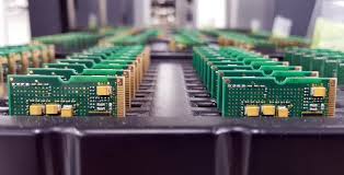
13. PCB Assembly (PCBA)
Once the bare PCB passes quality checks, it moves to the assembly phase, where components are soldered onto the board. This process includes:
- Surface Mount Technology (SMT) for automated component placement
- Through-hole soldering for components requiring extra mechanical support
- Reflow soldering and wave soldering for securing connections
14. Final Inspection and Quality Control
After assembly, PCBs undergo another round of inspections, including in-circuit testing (ICT) and functional testing, to ensure reliability and performance. Any defective boards are reworked or discarded.
15. Packaging and Shipment
Once the PCBs meet all quality standards, they are packaged using anti-static materials to prevent damage during transportation. PCBs are then shipped to manufacturers for integration into final products.
Conclusion
The PCB manufacturing process is a complex, multi-step procedure that requires precision and expertise. Choosing a reputable PCB manufacturer ensures that each step is carried out with accuracy, resulting in high-quality, durable PCBs for various applications. By understanding the process, engineers and designers can optimize their PCB designs for better functionality and cost efficiency.